Organic Electronic Technologies (OET)
About us
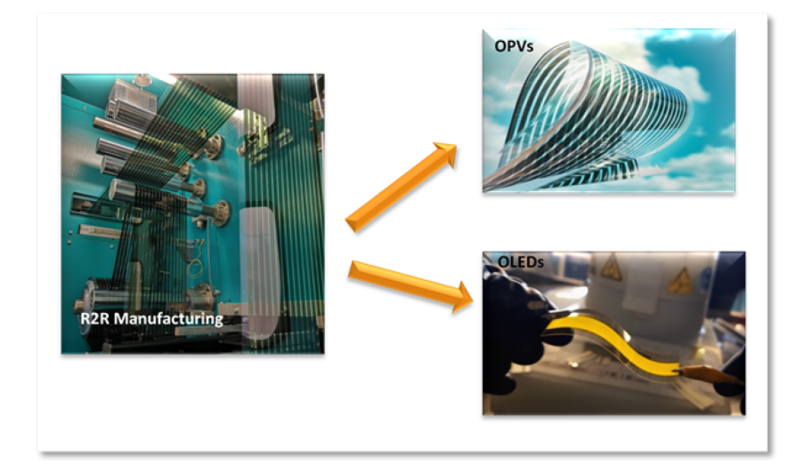
ΟΕΤ is a high-tech SME, founded in Thessaloniki in 2012 with an expertise in R2R manufacturing and technologies for flexible Organic Electronics (OE), holding more than 30 years of experience in thin film technologies and printed OEs. OET develops and optimizes unique, patented R2R manufacturing pro¬cesses and equipment (R2R printing, Laser patterning and Quality con¬trol tools) for Organic Printed Photovoltaics, Organic LED (OLED) and other OE products and applications. OET develops and optimizes the material formulations, thin films and process technologies for OE devices. Its expertise and know-how in¬cludes research and technology for design, manufacturing and applica¬tion of OPV and OLED products.
Our vision is “sustainable energy from every surface and everywhere” through the application of flexible, innovative Organic Printed Photovoltaics in buildings, facades, automotive and transport applications, tourism, greenhouses and wearable products. Our unique competencies include:
- R2R manufacturing and mass production of fully printed OPVs
- Process technologies and manufacturing automations for flexible OPVs and OLEDs
- In-line optical metrologies and methodologies and quality control tools for process reliability and manufacturability
- In-line Pulsed Laser patterning tools for minimal losses and high quality and performance devices at low T
- Turn-key Solutions for design and development of highly performing OPV and OLED applications.
ROLL TO ROLL (R2R) PRINTING
OET designs and develops R2R printing, pulsed laser processing and quality control technologies, aiming at cost-effective, high-throughput manufacturing of OPVs on flexible plastic surfaces. Its achievement in scalable production and nanoscale precision in R2R printing machines, optical engineering, reduction of manufacturing waste and costs, and increasing efficiency of OPVs is based on a huge R&D investment that took place during the last decade in developing R2R production line, unique in-line optical precision metrologies and quality control and pulsed laser scribing tools.
OPTICAL METROLOGY AND QUALITY CONTROL
OET devices consist of multilayer stacks, with a thickness ranging from a few to hundred nanometers, deposited by various printing processes onto flexible substrates of only 100μm thick. The major factors that affect the functionality of the deposited films, which are directly related to the OPV device performance, are their optical properties, uniformity, composition, morphology, nano-separation, surface roughness and thickness. Thus, in-line and real-time precision optical metrology and quality control of film deposition down to sub-nanometer scale is crucial for the process repeatability, reduction of waste and cost-effective manufacturing production. OET holds vast experience in developing and deploying patented In-line and In-situ Spectroscopic Ellipsometry (SE) in thin films precision metrology and OPV production. SE is a powerful and robust, non-destructive optical metrology tool for the real-time monitoring of the key layer properties that affect device quality, performance and process reliability. In-line metrology tools aid the real-time automated decision-making process based on digital closed loop feedback control that can lead to higher production yield, zero-defect manufacturing and product quality that meets the highest standards.
PULSED LASER PATTERNING
Ultra-Short, Pulsed Laser scribing is considered ideal for selective thin film (organic and inorganic) material removal and electrical isolation cuts, on rigid and flexible substrates, due to low temperature removal mechanism (Cold Ablation). OET provides the process technology platform for the optimization of in-line, micro-precision, pulsed laser scribing in production of OPVs to increase the active area and performance and by avoiding dangerous and toxic chemicals.


